- 您现在的位置:买卖IC网 > Sheet目录369 > W948D2FBJX5E (Winbond Electronics)IC LPDDR SDRAM 256MBIT 90VFBGA
�� �
�
�W948D6FB� /� W948D2FB�
�256Mb� Mobile� LPDDR�
�7.6.13� Interrupting� Write� to� Precharge�
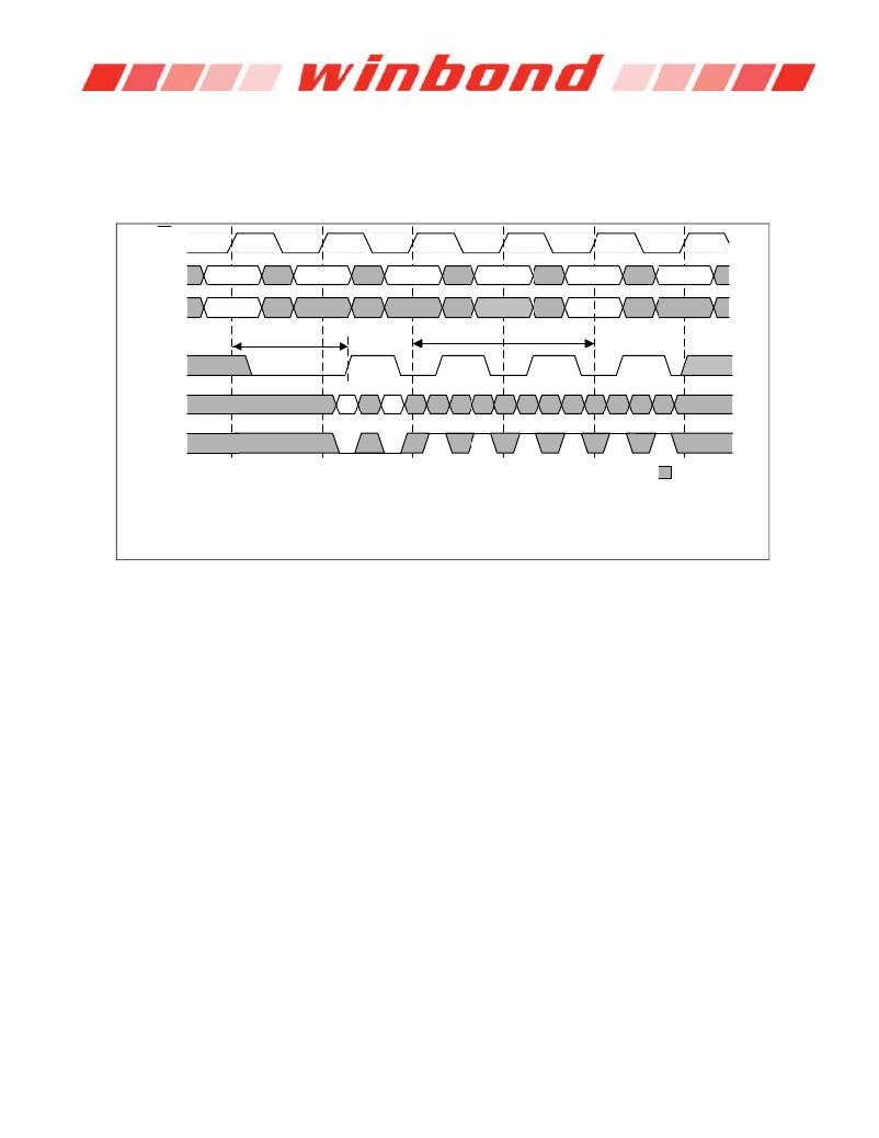
�Data� for� any� WRITE� burst� may� be� truncated� by� a� subsequent� PRECHARGE� command� as� shown� in� figure� below.�
�Note� that� only� data-in� pairs� that� are� registered� prior� to� the� t� WR� period� are� written� to� the� internal� array,� and� any�
�subsequent� data-in� should� be� masked� with� DM,� as� shown� in� figure.� Following� the� PRECHARGE� command,� a�
�subsequent� command� to� the� same� bank� cannot� be� issued� until� t� RP� is� met.�
�CK�
�CK�
�Command�
�WRITE�
�NOP�
�NOP�
�NOP�
�PRE�
�NOP�
�Address�
�BA,Col� b�
�BA,Col� n�
�BA� a(or�
�all)�
�DQS�
�DQ�
�t� DQSSmax�
�DI� b�
�t� WR�
�*2�
�DM�
�*1�
�*1�
�*1�
�*1�
�1)� Dl� b� =� Data� in� to� column� b.�
�=� Don't� Care�
�2)� An� interrupted� burst� of� 4,� 8� or� 16� is� shown,� 2� data� elements� are� written.�
�3)� t� WR� is� referenced� from� the� positive� clock� edge� after� the� last� desired� Data� In� pair.�
�4)� A10� is� LOW� with� the� WRITE� command� (Auto� Precharge� is� disabled)�
�5)� *1=can� be� Don't� Care� for� programmed� burst� length� of� 4�
�6)� *2=for� programmed� burst� length� of� 4,� DQS� becomes� Don't� Care� at� this� point�
�7.7� Precharge�
�The� PRECHARGE� command� is� used� to� deactivate� the� open� row� in� a� particular� bank� or� the� open� row� in� all� banks.�
�The� bank(s)� will� be� available� for� a� subsequent� row� access� a� specified� time� (t� RP� )� after� the� PRECHARGE� command� is�
�issued.�
�Input� A10� determines� whether� one� or� all� banks� are� to� be� precharged.� In� case� where� only� one� bank� is� to� be�
�precharged,� inputs� BA0,� BA1� select� the� bank.� Otherwise� BA0,� BA1� are� treated� as� “Don?t� Care”.�
�Once� a� bank� has� been� precharged,� it� is� in� the� idle� state� and� must� be� activated� prior� to� any� READ� or� WRITE�
�command� being� issued.� A� PRECHARGE� command� will� be� treated� as� a� NOP� if� there� is� no� open� row� in� that� bank,� or� if�
�the� previously� open� row� is� already� in� the� process� of� precharging.�
�Publication� Release� Date� :� Oct,� 15,� 2012�
�-� 39� -�
�Revision� :� A01-004�
�发布紧急采购,3分钟左右您将得到回复。
相关PDF资料
W949D2CBJX5E
IC LPDDR SDRAM 512MBIT 90VFBGA
W971GG6JB25I
IC DDR2 SDRAM 1GBIT 84WBGA
W971GG8JB-25
IC DDR2 SDRAM 1GBIT 60WBGA
W9725G6IB-25
IC DDR2-800 SDRAM 256MB 84-WBGA
W9725G6JB25I
IC DDR2 SDRAM 256MBIT 84WBGA
W9725G6KB-25I
IC DDR2 SDRAM 256MBIT 84WBGA
W972GG6JB-3I
IC DDR2 SDRAM 2GBITS 84WBGA
W9751G6IB-25
IC DDR2-800 SDRAM 512MB 84-WBGA
相关代理商/技术参数
W948D2FBJX5ETR
制造商:Winbond Electronics Corp 功能描述:256M MDDR, X32, 200MHZ
W948D2FBJX5I
制造商:Winbond Electronics Corp 功能描述:DRAM Chip DDR SDRAM 256M-Bit 8Mx32 1.8V 90-Pin VFBGA 制造商:Winbond Electronics Corp 功能描述:IC MEMORY
W948D2FBJX5I TR
制造商:Winbond Electronics Corp 功能描述:256M MDDR, X32, 200MHZ, INDUST
W948D2FBJX6E
制造商:Winbond Electronics Corp 功能描述:DRAM Chip DDR SDRAM 256M-Bit 8Mx32 1.8V 90-Pin VFBGA 制造商:Winbond Electronics 功能描述:LOW POWER DRAM 制造商:Winbond Electronics Corp 功能描述:IC MEMORY
W948D2FBJX6ETR
制造商:Winbond Electronics Corp 功能描述:256M MDDR, X32, 166MHZ, 65NM
W948D2FBJX6G
制造商:WINBOND 制造商全称:Winbond 功能描述:256Mb Mobile LPDDR
W948D6FB
制造商:WINBOND 制造商全称:Winbond 功能描述:256Mb Mobile LPDDR
W948D6FBHX5E
功能描述:IC LPDDR SDRAM 256MBIT 60VFBGA RoHS:是 类别:集成电路 (IC) >> 存储器 系列:- 标准包装:1 系列:- 格式 - 存储器:闪存 存储器类型:闪存 - NAND 存储容量:4G(256M x 16) 速度:- 接口:并联 电源电压:2.7 V ~ 3.6 V 工作温度:0°C ~ 70°C 封装/外壳:48-TFSOP(0.724",18.40mm 宽) 供应商设备封装:48-TSOP I 包装:Digi-Reel® 其它名称:557-1461-6